

Download all circuits from github
Introduction:
ISA (instruction set architecture) decides how to represent an instruction of a processor in Instruction memory, how the instruction is oriented, what is the length of an instruction, in which way the instruction should be decoded so that the CPU gets appropriate data. We already have our ISA. The objective is to design our processor based on the ISA. In this section, we have designed a 16 bit ALU, 16 bit Register File & a Control Unit. Then connected all the component with Program counter, Instruction Memory, Data Memory etc etc so that our processor works. Our Goal is to execute the 15 instructions (without multiplication) described in ISA successfully in our processor.
Arithmetic & Logic Unit (ALU):
ALU stands for “ARITHMETIC AND LOGIC UNIT” which does a bunch of arithmetic and logical operations. It is a very important hardware component of central processing unit of a computer. ALU is the main hardware part where the operations get executed. For our CPU, we will design an ALU which will be able to do Arithmetic Op – (Addition, Subtraction), Logical Op – (and, or, nor, xor).
To do add operation, we used carry look ahead adder. So that our adder won’t have any propagation delay. As our ALU will do operation with 16 bit data, logically we should build a 16 bit carry look ahead adder. But it will be very complex. So we built a 4 bit carry look ahead adder as a smallest unit adder and then added 4 adders of that unit to make a 16 bit adder. So that we could minimize the maximum propagation delay. Click here to see how to design 4 bit carry look-ahead adder.
Our smallest unit of adder is 4 bit. So, first of all we have built a 4 bit ALU which will do our necessary operations.
4 bit ALU Design:
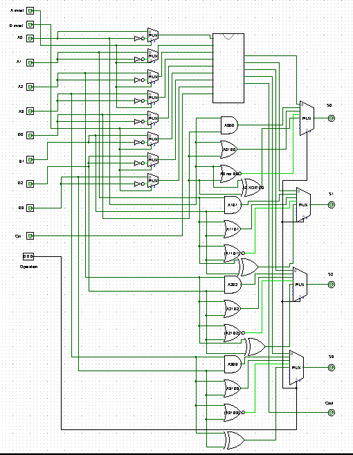
The square size sub-circuit in picture above is our designed 4 bit carry look-ahead adder. The ALU above will do our necessary operations for only 4 bit data (A0 A1 A2 A3, B0 B1 B2 B3). To get required operation, we have to change the select bit of our 8:1 MUX. The control bits are described below:
ALU Control Bits:
| Operation | Select Bit | A invert | B invert | Cin |
| Add | 000 | 0 | 0 | 0 |
| Sub (A-B) | 000 | 0 | 1 | 1 |
| Sub (B-A) | 000 | 1 | 0 | 1 |
| and | 001 | 0 | 0 | 0 |
| or | 010 | 0 | 0 | 0 |
| nor | 011 | 0 | 0 | 0 |
| xor | 100 | 0 | 0 | 0 |
Now, we have full-functional 4 bit ALU. We have to combine 4 unit of this 4 bit ALU to build a 16 bit ALU as we require. Circuit below is a 16 bit ALU built with four 4 bit ALU sub-circuit. Additionally we have connected all the 16 result bit in a nor gate. We will see the function of this nor gate later.
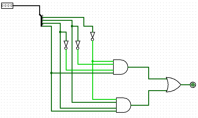
16 bit ALU:
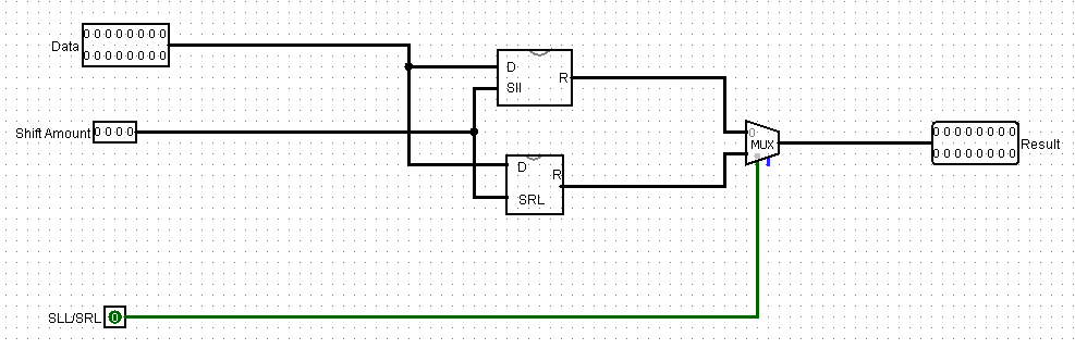
Shift Right Logical & Shift Left Logical Circuit Design:
Our smallest unit of the ALU is 4 bit. And we combined those 4 bit ALU’s to build a 16 bit ALU. For this designing purpose, we can’t include shift logical circuits inside ALU. But our processor have to do SLL & SRL operations. So, we have separated SLL & SRL circuit from ALU and putted it outside ALU.
According to our ISA, SLL and SRL operations are immediate type operation. We will have 4 bit immediate value which will tell how much to shift left/right.
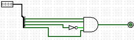
SLL Circuit:

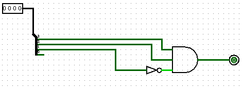
SRL Circuit:
![]()
SLL & SRL:
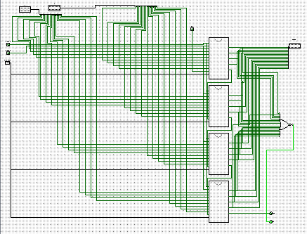
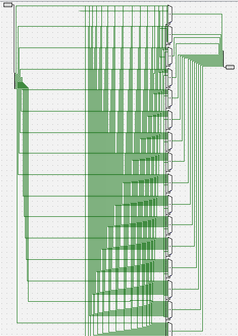
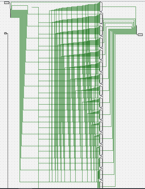
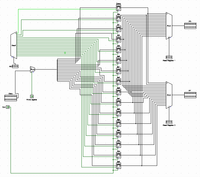
Register File:
In processor, ALU gets data from a Register Bank / Register File. As we have designed our ISA, our register file should have 16 registers. And the design should be easy enough to choose rs, rt, rd values. The circuit below is our register file design. Note: each register is able to store 16 bit data.
Register File Design:
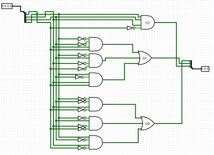
Control Unit:
Control unit is the circuit in processor which controls the flow of data and operation of ALU. Initially an instruction is loaded in instruction memory. According to Opcode of that instruction, control unit gets understood what the instruction wants to execute. Then it flows the data in such a path so that ALU gets necessary data to execute.
Control unit design:
As our designed ISA, our CPU should be able to do 15 operations. The table below represents a demo of 15 operations, binary form of the operations following our ISA design & hex form of the operation.
Instructions Demo:
| MIPS CODE | Binary String | Hex Code |
| add $s1 $t0 $s2 | 0000 0001 0111 0110 | 176 |
| sub $s3 $t2 $t1 | 0001 0011 0010 1000 | 1328 |
| and $s4 $t0 $t1 | 0010 0001 0010 1001 | 2129 |
| or $s5 $t0 $t1 | 0011 0001 0010 1010 | 312A |
| nor $s0 $t0 $t1 | 0100 0001 0010 0101 | 4125 |
| addi $s1 $t1 4 | 1001 0010 0110 0100 | 9264 |
| andi $s2 $t1 4 | 1010 0010 0111 0100 | A274 |
| ori $s3 $t1 4 | 1011 0010 1000 0100 | B284 |
| lw $s4 3($t2) | 0101 0011 1001 0011 | 5393 |
| sw $s0 2($s1) | 0110 0110 0101 0010 | 6652 |
| xor $s1 $t1 $t2 | 1110 0010 0011 0110 | E236 |
| beq $t0 $t2 0001(L)
add $s1 $t0 $s2 L: sub $s3 $t2 $t1
[L = address of instruction – 1] |
0111 0001 0011 0001 | 7131
176 1328 |
| J 4 | 1111 000000000100 | F004 |
| sll $so $to 4 | 1100 0001 0101 0100 | C154 |
| srl $so $to 4 | 1101 0001 0101 0100 | D154 |
To execute these instructions, some bits should be 0/1 according to necessity of data-path flow. You can take a look how this circuit’s Data-Path works. The table below describes which instruction needs which bit to be 0/1.
Control Table: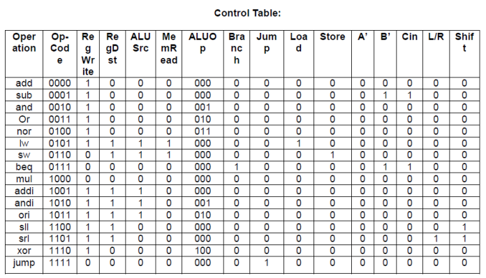
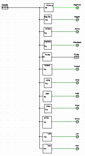
Following this control table, we built circuits for RegWrite, RegDst, ALUSrc, MemRead, ALUOp, Branch, Jump, Load, Store, A’, B’, Cin, L/R, Shift. Minimized with K-map when needed.
Regwrite:
RegDst:
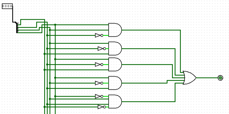
ALUSrc:
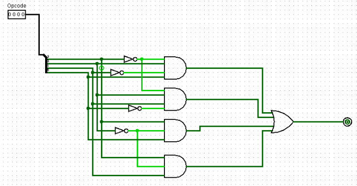
MemRead:
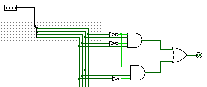
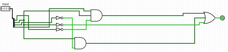
ALUOp:
Branch:
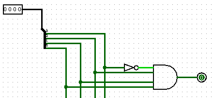
Jump:
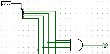
Load:
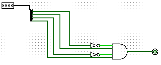
Store:
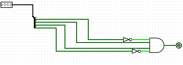
B’/Cin:
L/R:
Shift:
Control Unit Circuit:
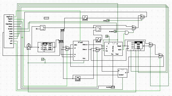
Processor Circuit:
Now, connect ALU, Register file, Instruction Memory, Data Memory, control unit and all other hardwires to complete the design. The circuit below is our complete 16 bit processor according to our ISA design.
Conclusion:
The processor is able to successfully execute the 15 operations from ISA design. It can’t execute only multiplication. To execute any instruction, the syntax and the orientation of different type of instructions explained in ISA must be followed. Otherwise the CPU won’t work properly.

2 Pingback